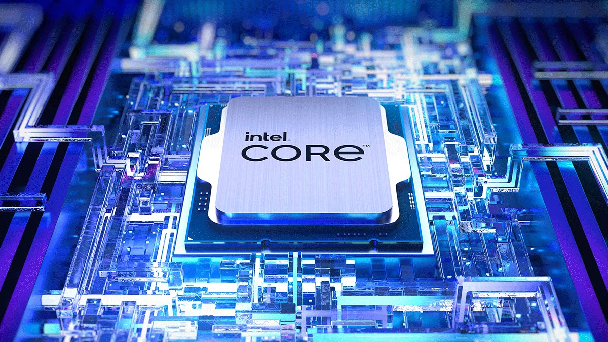
Building a modern electronic device means packing an entire computer onto a single piece of silicon. This approach, known as a System-on-Chip (SoC), integrates processing cores, memory controllers, graphics engines, and input-output interfaces onto one microchip. Instead of wiring discrete components across a bulky motherboard, engineers rely on SoC designs to shrink footprint size, slash power consumption, and speed up data transfer for devices ranging from smartphones to automotive ECUs.
Traditional circuit boards required separate chips for the processor, memory, and peripheral controllers, which introduced noticeable latency and high power loss as signals traveled across board traces. SoC architecture eliminates these bottlenecks by placing everything on a single die or within a multi-die package. Signals travel mere micrometers rather than centimeters, which changes how devices manage heat, battery life, and processing throughput.
Core Components of SoC Architecture
An SoC isn't a single monolithic block; it's a complex collection of intellectual property (IP) blocks combined via on-chip interconnects. Understanding how these blocks interact is essential for hardware engineers.
Processing Units and Compute Engines
The processing core acts as the computational engine. Most modern designs combine central processing units (CPUs) for sequential control tasks with specialized processors like graphics processing units (GPUs) for parallel rendering. Many architectures also incorporate neural processing units (NPUs) built specifically to handle machine learning matrix multiplications without draining the primary CPU.
Memory Subsystems and Caches
Data movement dictates overall system performance. SoCs utilize a hierarchical memory model featuring ultra-fast L1, L2, and L3 on-chip static RAM (SRAM) caches tied directly to the execution cores. For bulk storage and runtime memory, the SoC interfaces with external dynamic RAM (DRAM) using high-bandwidth memory controllers that support standards like LPDDR5.
On-Chip Interconnects
Moving data between dozens of independent IP blocks requires robust internal highways. Modern chips move away from traditional shared buses toward Network-on-Chip (NoC) architectures. A NoC uses packet-switched routing networks to move data packets across the silicon die efficiently, preventing traffic jams between the processor, memory, and peripherals.
Power Management Units
Thermal regulation and energy conservation dictate chip viability in mobile and edge deployments. The power management unit (PMU) controls voltage scaling, clock gating, and power domains. It shuts down inactive blocks instantly to preserve battery life and prevent thermal throttling.
The SoC Design Flow
Designing a functional silicon chip takes years of planning, simulation, and verification. Teams follow a strict workflow to move from abstract concepts to physical manufacturing masks.
Architectural Specification and IP Selection
Engineering teams begin by defining performance targets, power envelopes, and cost constraints. They license pre-designed IP blocks—such as ARM Cortex cores or proprietary GPU blocks—rather than building every component from scratch.
Register-Transfer Level Design and Synthesis
Engineers write hardware description languages like Verilog or SystemVerilog to define how data moves through registers and logic gates. Synthesis tools translate this code into a gate-level netlist optimized for specific performance metrics.
Physical Implementation and Verification
The netlist undergoes placement and routing, where software maps logic gates onto physical silicon coordinates. Engineers run rigorous timing analysis, power simulations, and design rule checks to ensure the chip will function correctly under real-world conditions. Once verified, the design goes to a semiconductor foundry for tape-out and fabrication.
Key Engineering Challenges
Building dense silicon chips brings severe physical and logical hurdles that demand constant innovation.
Thermal Dissipation and Dark Silicon
As transistor density increases, heat builds up faster than it can escape. Engineers face the reality of "dark silicon," where portions of the chip must remain powered off at any given time to prevent the processor from overheating.
Verification Complexity
Verification consumes up to seventy percent of a chip development project. Ensuring that millions of logic gates interact flawlessly without deadlocks or race conditions requires advanced emulation platforms and automated testbench generation.
Process Node Scaling Limits
Moving down to smaller manufacturing nodes, such as 3nm and 2nm processes, introduces quantum tunneling effects, manufacturing defects, and skyrocketing mask costs. Designing chips at these scales requires radical shifts in physical geometry and packaging techniques.
Modern Trends in Semiconductor Design
The industry is shifting away from monolithic chips toward advanced packaging techniques to bypass the physical limits of single-die scaling.
Heterogeneous Integration and Chiplets
Instead of cramming every feature onto one massive piece of silicon, manufacturers split designs into smaller functional chiplets. These chiplets connect via high-density interposers in a 2.5D or 3D package, combining different manufacturing nodes on a single substrate.
Edge Artificial Intelligence Integration
Hardware acceleration for machine learning is no longer optional. Modern chips embed dedicated tensor processing blocks directly into the SoC fabric, allowing devices to run computer vision and natural language processing locally without relying on cloud data centers. Learn more about advanced semiconductor manufacturing trends at IEEE Spectrum.
Frequently Asked Questions
What is the difference between a CPU and an SoC?
A CPU is a single processing component that executes instructions. An SoC is an entire system on a single chip that includes a CPU, GPU, memory controllers, input-output interfaces, and power management units.
Why are modern chips moving toward chiplet designs?
Monolithic chips become exponentially more expensive and prone to manufacturing defects as they grow larger. Chiplet designs break the system into smaller, modular dies, improving manufacturing yields and reducing costs.
How do SoCs manage heat generation?
SoCs use dynamic voltage and frequency scaling, clock gating, and thermal sensors. When a region gets too hot, the power management unit lowers clock speeds or shuts off idle power domains.
What role do hardware description languages play in design?
Languages like Verilog and VHDL allow engineers to describe circuit behavior and logic structures using code, which synthesis tools then convert into physical silicon layouts. For official documentation on semiconductor standards, visit Accellera Systems Initiative.